Making a Raspberry Pi Pico (RP2040) PCB as a beginner [DRAFT]
Making an "real" PCB has always felt like magic to me. I decided to give it a go given how cheap it is with the chinese PCB houses. A few of my colleagues had used JLC previously, so I decided to go with them as well. Please note that these are beginners notes, this is what I did - best practices for someone who knows what they are doing are most likely going to be significantly different.
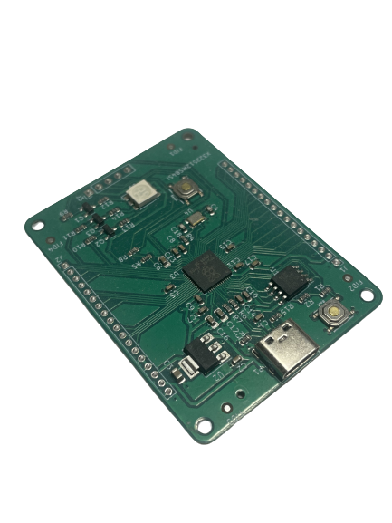
In the end, this is what I ended up with: And yes, it works:

Why not just buy a finished board?
Yes, that would be the sensible thing to do. This board is larger, more expensive and really doesn't add anything. But I wanted to make my own.
Documentation
The Raspberry Pi foundation has published fantastic documentation on how to design a board using the RP2040 which I used extensively. It was understandable even as a beginner to PCB design.
Component selection
I tried as far as possible to use components available in the JLCPCB "basic components" bin. There's a $1 fee for every non-basic component (for loading the pick and place machine I presume) when you order assembled PCBs.
USB/power
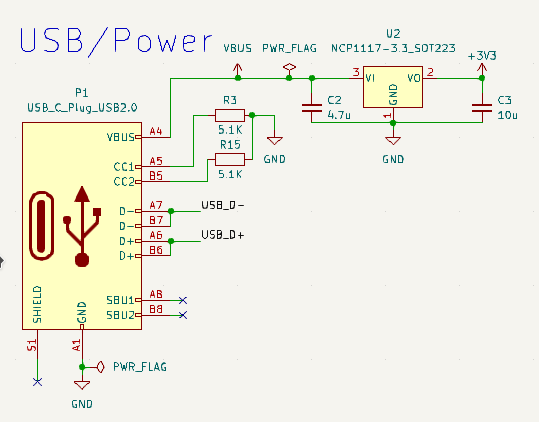
The RP2040 only needs a +3.3V supply, generating other needed voltages internally. I chose a NCP1117 as a simple linear voltage regulator that was available as a basic part, and could provide 1A which should be plenty for a simple development board like this. It's not very good when it comes to standby power consumption, but that's not something I cared about here.
I wanted a USB-C plug even though Micro-USB was significantly cheaper, because, well, it felt more modern. There's a simplified plug with only USB2.0 connection, making sure I didn't need to worry about all fancy USB 3.0+ stuff. Because USB-C is a reversible connector, all signals are duplicated:

The pins I needed to care about here to act as a USB 2.0 device:
D-(A6 and B6) andD+(A7 and B7) - The USB2.0 data differential pair. The duplicated pins are connected together.CC1andCC2- Can be used to detect orientation, cable attachment and removal and current negotiation. Fortunately, there's a simplified way for basic use: use 5.1K pulldown resistors on each CC pin to signal 5V up to 3A (and hope the power supply can deliver that).VBUS- Positive voltage. All four pins are connected together.GND- Ground. All four pins are connected together.SBU- Leave unconnected
This is the schematic I ended up with:

Flash storage, boot and reset
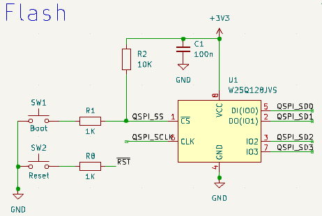
I used a Winbond W25Q128JVS 16 MB Quad-SPI NOR flash chip. Quad-SPI as you might guess imply there are for pins for data, IO0-3. The boot switch button pulls chip-select to low, otherwise it's held high by R2.

Layout

Notes for the future
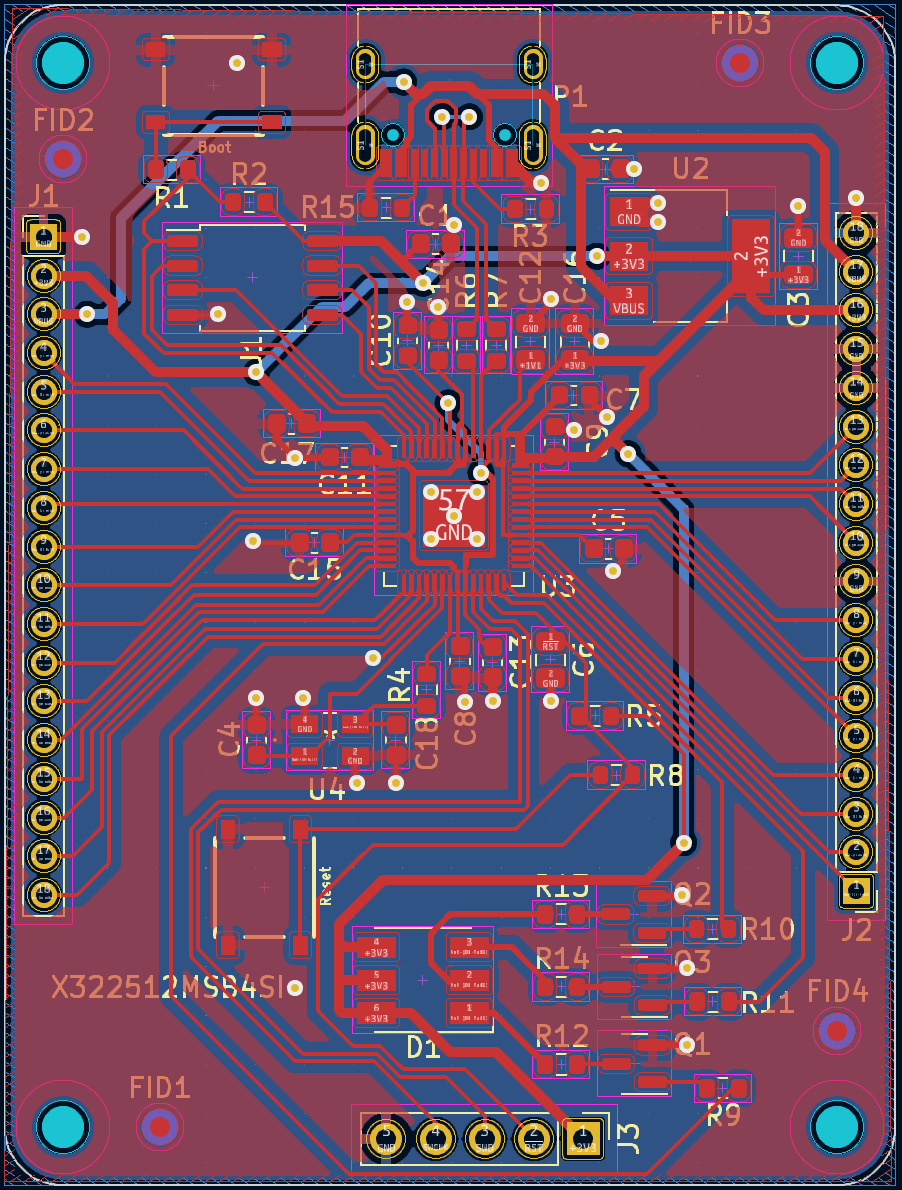
- I used the wrong pin headers for the GPIO pins, I intended to use standard 2.54 mm (0.1 in) connectors but accidentally chose the less common metric 2.00 mm header instead. I didn't notice until I got the boards back.
- I should have labeled each pin header on the silk screen. I knew this. I was just lazy, and now I need to go back to the schematic and trace back what each pin is when I want to use my PCBs (which is way more work).
- PCBs without connectivity are of limited use. I usually end up using a cheap ESP8266 or ESP32 for other projects instead just because they have wifi. I wonder if there are any easy to use and obtain wifi chips suitable for DIY use? Please let me know if you know of any.
Next: HlK-LD2410C radar presence sensors, MQTT and home assistant [DRAFT]